From an Idea to a Product: Trying, Testing, Optimizing
SCHREINER LOGIDATA
From an Idea to a Product:
Trying, Testing, Optimizing
Customized products and solutions are a specialty of Schreiner Group and the field in which the experts at the Schreiner LogiData competence center are active. So, what are the requisite steps to turn an initial idea into a real product? Here’s a brief look at the work of the RFID developers.
The small coffee corner on the second floor is something like an unofficial, creative communications center. Because even though the final fine-tuning takes most of the time in the development process chain, Hartmut Wiederrecht, the leader of the RFID development team at Schreiner LogiData, puts the situation in a nutshell: “Without the spark of an idea you’ve got nothing.”
A total of three product developers and three process developers are currently engaged in the complex process of developing RFID inlays. An inlay not only consists of the RFID chip but also of the antenna. Because Schreiner Group has increasingly evolved into a supplier of customized solutions the work includes not only a high level of technical knowledge and experience but also plenty of creativity. And that’s exactly what makes our job so attractive, says Wiederrecht: developing something that doesn’t exist on the market yet exactly according to the customer’s wishes and requirements.
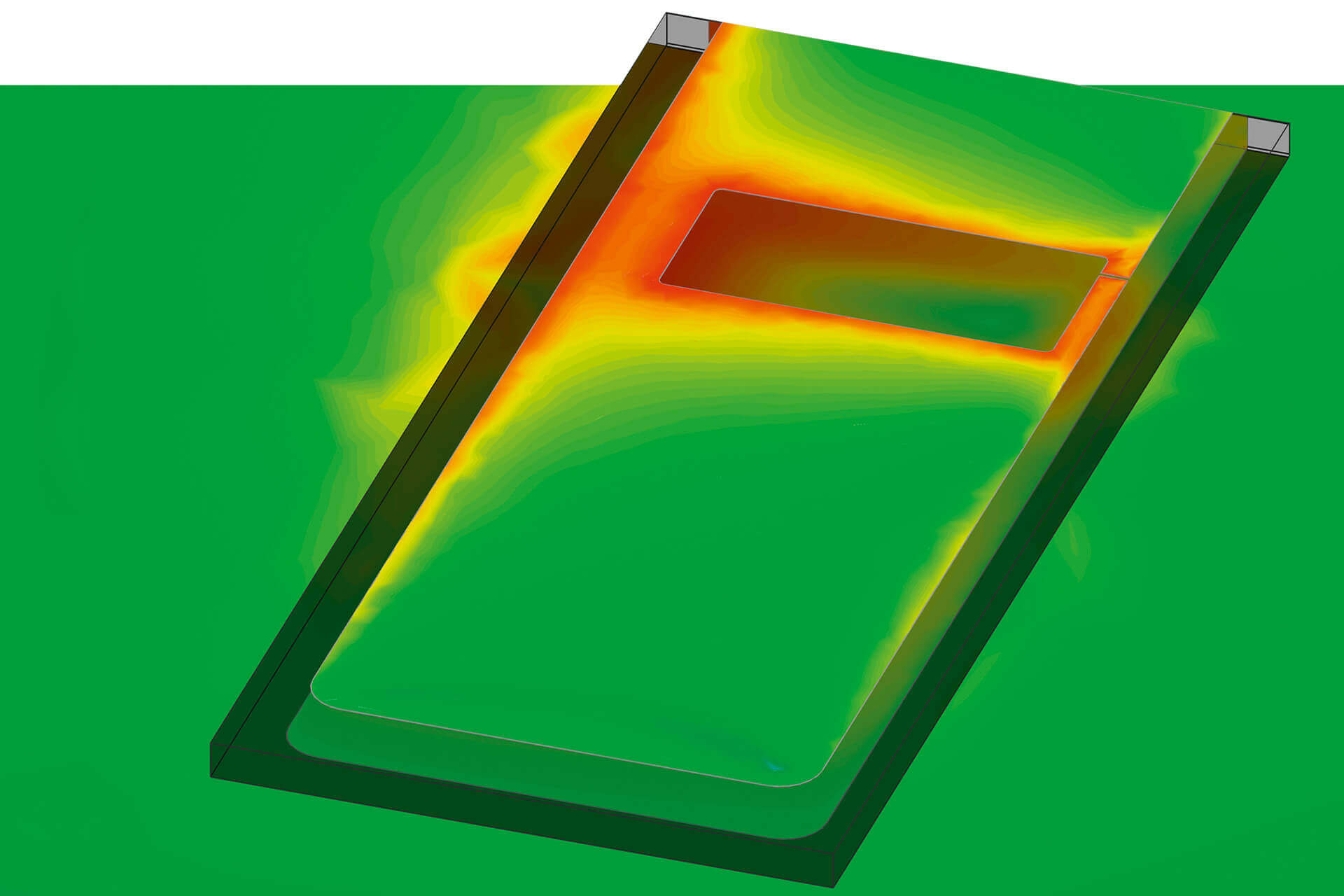
Once the developer’s initial idea has been realized considering factors like size, shape, and operating conditions, the finalization stage begins. It involves the specific design of the antenna and selection of the chip. The required frequency, desired read range, and the necessary storage capacity are fed into the process at that time. For the developer, that means it’s time to boot the PC!
With the help of simulation software, the expert can simulate the relevant ambient conditions and other details. The simulation incorporates the key aspects of the customer’s real-world environment that will affect the performance of the RFID label. “That’s the major advantage of a simulation calculation,” says Wiederrecht. “You can come very close to the final design without the complex need of having to make a real-world sample. In addition, you can find out very fast what impact the change of a parameter has on the inlay and in that way optimize it step by step.
The best three concepts are turned into prototypes. To enable quick response in development projects, Schreiner Group has an in-house system for making RFID inlays. The next stage is the measuring chamber. These tests are also performed on the customer’s real objects in order to consider the future ambient conditions and ensure that the RFID inlay optimally conforms to the respective requirements. In that stage, several variants are made again from which the best one can be selected. Finally, the inlay with optimal characteristics can go into mass production.

By the way, the information gained from the test runs is fed back into the simulation software. That helps create increasingly better databases for future development projects which in turn leads to continuous improvements of the simulation results—thus increasingly approaching the real-world inlay.
Whether round, angular, with first-opening indication, for metallic substrates, or for curved objects: The development of RFID inlays is a challenging process for which careful planning, design and production processes are of crucial importance to ensure that the final product will meet the customer’s needs. For the team from Schreiner LogiData that means sustaining its know-how on a high level, continuing to advance RFID technology, and opening up new fields of application: with plenty of competence, creativity—and certainly an occasional cup of coffee.


